.svg)
.svg)

.svg)

ترجمه مقاله یک مقایسه کننده دیفرانسیلی توان پایین و سرعت بالا برای مبدل های آنالوگ به دیجیتال - نشریه IEEE

عنوان فارسی
یک مقایسه کننده دیفرانسیلی توان پایین و سرعت بالا با آفست کم، برای مبدل های آنالوگ به دیجیتال
عنوان انگلیسی
A High-Speed, Low-Offset and Low-Power Differential Comparator for Analog to Digital Converters
صفحات مقاله فارسی
6
صفحات مقاله انگلیسی
2
سال انتشار
2017
رفرنس
دارای رفرنس در داخل متن و انتهای مقاله
نشریه
آی تریپل ای - IEEE
فرمت مقاله انگلیسی
PDF
فرمت ترجمه مقاله
pdf و ورد تایپ شده با قابلیت ویرایش
فونت ترجمه مقاله
بی نازنین
سایز ترجمه مقاله
14
نوع مقاله
ISI
نوع ارائه مقاله
کنفرانس
کد محصول
10845
وضعیت ترجمه عناوین تصاویر و جداول
ترجمه شده است ✓
وضعیت ترجمه متون داخل تصاویر و جداول
ترجمه نشده است ☓
وضعیت ترجمه منابع داخل متن
به صورت عدد درج شده است ✓
وضعیت فرمولها و محاسبات در فایل ترجمه
به صورت عکس، درج شده است
ضمیمه
ندارد ☓
بیس
نیست ☓
مدل مفهومی
ندارد ☓
پرسشنامه
ندارد ☓
متغیر
ندارد ☓
رفرنس در ترجمه
در داخل متن و انتهای مقاله درج شده است
رشته و گرایش های مرتبط با این مقاله
مهندسی برق، مهندسی الکترونیک، سیستم های قدرت، سیستمهای الکترونیک دیجیتال
کنفرانس
کنفرانس بین المللی طراحی SoC
دانشگاه
گروه مهندسی برق، دانشگاه ایالتی سن خوزه، ایالات متحده آمریکا
کلمات کلیدی
مقایسه کننده سرعت بالا، آفست کم، توان پایین، نویز kickback پایین
کلمات کلیدی انگلیسی
High speed comparator - low offset - low power - low kickback noise
doi یا شناسه دیجیتال
https://doi.org/10.1109/ISOCC.2017.8368862
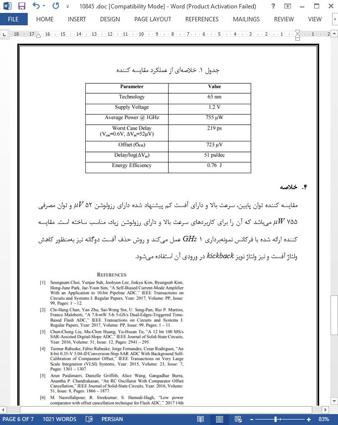
۰.۰
(هنوز امتیازی ثبت نشده است)