Abstract
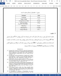
Analysis and design of a high-speed comparator with improved input referred offset is presented in this paper. The proposed comparator is designed in TSMC low power CMOS technology under 1.2 V power supply. The new presented comparator has a low power consumption and utilizes dual offset cancellation technique. The minimum convertible input voltage is calculated to be 52 μV and the propagation delay at this worst case is equal to 219 ps. The power consumption at 1 GHz clock frequency is 755 μW. Monte Carlo simulation with 500 points iteration shows that the standard deviation of the input referred offset is about 723 μV.
I. INTRODUCTION
Comparators play the most important role in voltage based analog to digital converters (ADCs) such as successive approximation register (SAR), Pipeline, and specifically in Flash ADCs [1-3]. Designing the comparators in the lower power supply with higher speed and lower power has its own challenges. Besides, realizing circuits in sub-nano CMOS technologies need digitally assisted circuits and complex techniques to overcome the kickback noise and offset voltage [4- 6]. The kickback noise and offset variation due to the capacitive path to the input can degrade the overall performance of the system, e.g., it can shift the different reference voltage levels in Flash ADC. This degradation will result in the erroneous conversion process.
IV. SUMMARY
The proposed high-speed, low-offset, low-power comparator has a resolution of 52 ȝV and a power consumption of 755 ȝW which make this comparator suitable for high resolution and fast applications. The presented comparator works with a 1 GHz sampling frequency where a dual offset cancellation technique is applied to reduce the offset voltage and kickback noise voltage to the input.


